Gigabit Networking Technology
Click here to find out about
Washington University's Gigabit Network Technology Distribution Program.
 Washington University's Applied Research Lab has designed a gigabit
ATM switch architecture and supporting chip set that supports the economical
construction of large-scale ATM switches with link speeds from 150 Mb/s
up to 2.4 Gb/s. It seeks to license this technology to commercial
organizations for use in state-of-the-art products that offer unique
advantages to customers. This chip set implements a patented architecture
(U.S. patent #5,402,415, March 28, 1995) that provides nearly flat cost
per port across a very wide range of system configurations (a system with
4096 ports of 2.4 Gb/s each has a cost per port only 20% higher than a
system with eight ports) and offers unsurpassed efficiency and flexibility
in the provision of switched multicast.
Washington University's Applied Research Lab has designed a gigabit
ATM switch architecture and supporting chip set that supports the economical
construction of large-scale ATM switches with link speeds from 150 Mb/s
up to 2.4 Gb/s. It seeks to license this technology to commercial
organizations for use in state-of-the-art products that offer unique
advantages to customers. This chip set implements a patented architecture
(U.S. patent #5,402,415, March 28, 1995) that provides nearly flat cost
per port across a very wide range of system configurations (a system with
4096 ports of 2.4 Gb/s each has a cost per port only 20% higher than a
system with eight ports) and offers unsurpassed efficiency and flexibility
in the provision of switched multicast.
Features and Capabilities
Washington University's Gigabit Switch (WUGS) technology has a variety of
features
that make it ideally suited to the construction of large, economical and
high performance ATM networks.
- High performance components enabling port speeds up to 2.4 Gb/s.
This enables demanding applications that are beyond the reach of
lower speed systems and enables highly
efficient statistical multiplexing of more typical applications
with peak data rates from 1 to 100 Mb/s, greatly reducing the cost of
transmission in both local and wide area environments.
- Optimally efficient multicast switching. Our patented
multicast switching technique has optimal complexity in terms
of both the switching network and multicast routing memory, giving
it essentially constant per port costs for configurations ranging
from 8 to 4096 ports and throughputs approaching 10 Tb/s. This allows
large networks to be implemented at a fraction of the cost required
when using smaller switches.
- Efficient handling of many-to-many and many-to-one multicast.
Unlike standard ATM, the WUGS switch can support many-to-many and
many-to-one applications directly, rather than requiring
one-to-many overlays. This avoids the quadratic scaling
limitations inherent in the overlay method. Many-to-many
applications requiring explicit in-band sender identification can be
supported via end-to-end multicast virtual paths with the
virtual circuit identifier used for sender identification.
- Fast reconfiguration of multicast connections.
In previous ATM switch architectures, the time required to add or
remove an endpoint from a multicast connection grows with the size
of the switch and/or the connection. The WUGS architecture allows
constant time addition and removal of endpoints, allowing highly
dynamic multicast applications in which endpoints come and go
thousands of times per second.
- Effective packet-level discarding for gigabit links.
The WUGS switch employs an efficient variation of the early
packet discard technique that ensures that during overload, the
full link capacity is used for complete AAL-5 frames, not
fragments. Our technique adds hysteresis to the early packet
discard control algorithm, allowing it to achieve ideal throughput
with much smaller buffers than are needed otherwise.
Scalability -- Why Does It Matter?
As stated above, one of the distinguishing features of the WUGS switch
architecture is its cost-effectiveness in a wide range of system
sizes; but why are large switching systems of value in the first
place? One can obviously construct networks of arbitrary size using
switches with modest numbers of ports, so why should one bother with
large switches? The answer to this is that large switches have an
inherent cost and performance advantage when it comes to building large
networks. This can be seen best by way of an example. Consider a typical
campus network of the future with 8,000 workstations and servers
connected to an ATM network with access links of 150 Mb/s. If we are
limited to switches with say 16 ports, we need to define an appropriate
interconnection topology to link these users together.
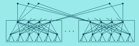
The figure at right shows an efficient general interconnection topology
that can be used for this purpose. If the access switches (the ones
connecting to the end systems) are configured so that the number of
ports connecting to other switches equals the number connecting to
end-systems (a 1:1 concentration ratio), then the total number of ports
on all the switches is seven times the number of users. For efficient
switch architectures, the total system cost is dominated by the per
port cost, making the cost of this hierarchical network roughly seven
times that for a single large switch. The following plots show how
this small switch penalty is affected by the total number of
users and the concentration ratio.
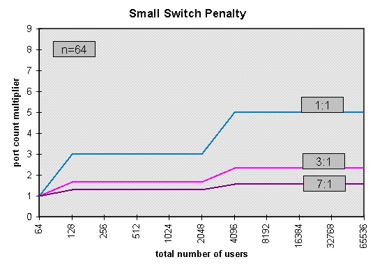
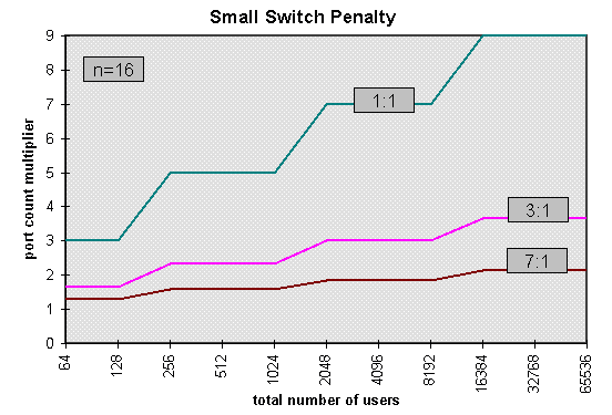 In these figures, the vertical axis shows the ratio of the total number
of switch ports required, to the number of users.
It takes large concentration ratios to reduce the small switch penalty
to a tolerable level. In addition to having a higher cost, the
hierarchical network design yields greatly inferior performance with
respect to virtual circuit blocking, queueing delay and cell loss even
with a 1:1 concentration ratio. Its blocking performance is
particularly poor for multicast connections.
In these figures, the vertical axis shows the ratio of the total number
of switch ports required, to the number of users.
It takes large concentration ratios to reduce the small switch penalty
to a tolerable level. In addition to having a higher cost, the
hierarchical network design yields greatly inferior performance with
respect to virtual circuit blocking, queueing delay and cell loss even
with a 1:1 concentration ratio. Its blocking performance is
particularly poor for multicast connections.
Who Needs Gigabit Links?
The importance of gigabit links is often attributed solely to their
role in supporting high speed applications. Equally (or more) important
is their role in lowering system costs through improved statistical
multiplexing and more efficient use of fiber. Consider, for example, a
collection of on-off bursty sources with a peak rate of 50 Mb/s and an
average rate of 2 Mb/s. On a 150 Mb/s link, we can multiplex at most 12
such virtual circuits before the probability of congestion (that is the
probability that any given virtual circuit encounters congestion when
it sends a burst of data) exceeds 1%. This gives a link efficiency of
16%. A 2.4 Gb/s link can handle 841 such virtual circuits before the
congestion probability exceeds 1%, giving an overall link efficiency
of 70%. For typical component costs today, this gives the 2.4 Gb/s
link a 5-to-1 cost/performance advantage over the equivalent collection
of 150 Mb/s links in short distance applications. In long distance
applications, where the fiber savings play a dominant role, the
advantage is much larger: 60-to-1 for a 50 mile link!
System Overview
The figure below shows the overall organization of the WUGS
switching system.
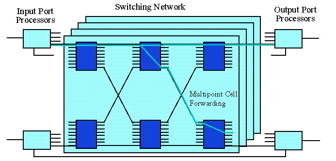
It consists of three
main components, which are each implemented as a single custom
integrated circuit. The Input Port Processors (IPP) at left,
receive cells from the incoming links, buffer them while awaiting
transmission through the central switching network and perform the
virtual path/circuit translation required to route cells to their proper
output (or outputs). The Output Port Processors resequence cells
received from the switching network and queue them while they await
transmission on the outgoing link. Each OPP is connected to its
corresponding IPP, providing the ability to recycle cells belonging to
multicast connections. This is discussed in more detail below. The
central switching network is made up of Switching Elements (SE)
with eight inputs and outputs and a common buffer to resolve local
contention. The SEs switch cells to the proper output (or outputs)
using information contained in the cell header
or can distribute cells dynamically to provide load balancing.
The load balancing option is used in the first
k-1 stages of a 2k-1 stage
network. In particular, for the configuration shown above
(k=2), load distribution is performed in the
first stage. Adjacent switch elements employ a simple hardware flow
control mechanism to regulate the flow of cells between successive
stages, eliminating the possibility of cell loss within the switching
network. With this approach, relatively small buffers suffice within
the network. Larger buffers are provided at the OPPs.
To provide sufficient bandwidth for 2.4 Gb/s data rates on the
external links, the switch carries ATM cells in a 36 bit wide format.
Four of the 36 bits contain addressing information and the remainder
contains the cell payload, together with auxiliary fields that are
added by the IPPs and removed by the OPPs. The internal cell cycle is
16 clock ticks long and the clock frequency used is 120 MHz. This
yields an internal cell processing rate that is about 1.3 times the
cell processing rate for external links operating at 2.4 Gb/s. The
switching network is implemented in four parallel planes, with each
plane receiving the same four bits of address information, plus eight
bits of data. The core of the system operates fully synchronously, and
the switch elements' operation is completely deterministic, meaning
that the cells proceed through the four planes in parallel, without any
explicit coordination, and are reconstructed at the OPP.
Switching Network
The switching network uses a Benes network topology. The Benes network
extends to arbitrarily large configurations by way of a recursive
expansion. The chip set generalizes the standard Benes network topology
to allow construction of switches in which the number of ports can be
any power of 2. Multistage switching networks with shared buffer
switch elements and interstage flow control can achieve high
throughputs with modest buffer capacities. In particular, the gigabit
switch technology can support fully loaded external links under uniform
random traffic. Bursty traffic requires some reduction in the average
link loading to achieve acceptable congestion probabilities on the
external links. For on-off virtual circuits with peak rates of 50 Mb/s
and a peak-to-average ratio of 10:1, the probability of output link
congestion is about .005 when the average link occupancy is 70%. At
this load, the probability of congesting the switching network is
.0001. At an average link occupancy of 50%, the corresponding
probabilities of congestion are one in a million and five in a billion,
respectively.
Using Cell Recycling for Multicast
The WUGS switch implements multicasting using a technique called
cell recycling. When cells arrive on an input link, the virtual path
and virtual circuit identifiers are used to select an entry from a
routing table in the IPP (called the Virtual Path/Circuit
Translation Table (VXT)). The entry includes a pair of output port
numbers, a pair of new virtual path and circuit identifiers and a pair
of control bits. The switching network routes a copy of the cell to
each of the designated outputs, where they can be forwarded to the
outgoing link or optionally recycled back to the input ports (this
choice is determined by the control bits), where the virtual path and
circuit identifiers are used to perform new VXT lookups, yielding new
pairs of destinations. Through this process, a connection with f
destinations can be handled in log2(f) passes through the network.
The combination of this technique with a
buffered multistage switching network using dynamic routing, yields
optimal cost/performance scaling, with respect to both the switching
network complexity and the amount of routing memory required. While the
recycling technique adds some delay, the absolute magnitude is small:
under 10 microseconds per pass for a switch with up to 4096 ports.
Because the cell recycling technique consumes a part of the system's
bandwidth to handle multicast connections, engineering rules are
needed to specify how much of the system's capacity to set aside for
multicast. In a system with n ports, we can
avoid blocking new connection requests if we dedicate a certain fraction
of the ports for
recycling. The figure below plots the fraction of ports that must be
dedicated to recycling under a wide range of conditions. It's important
to note that the fraction of the system's capacity that must be
dedicated to multicast is independent of the number of ports.
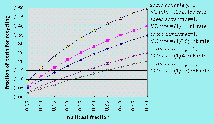
The plot gives the fraction of the total outgoing traffic that belongs
to multicast connections on the x axis and the fraction of the
switch's ports that must be dedicated to multicast to ensure that virtual
circuit blocking does not occur, on the y axis.
The different curves reflect different aspects of the system configuration.
In particular, the speed advantage is the ratio of the speed of the switch's
internal data paths to the speed of the external links (1 if all external
links operate at 2.4 Gb/s, 2 if they operate at 1.2 Gb/s).
For systems in which the external links can be fully loaded, but the
end users are limited to individual virtual circuit rates of 150 Mb/s,
the middle curve is the relevant one. Note that if 20% of the traffic
can be multicast, fewer than 20% of the switch ports must be dedicated
to recycling. Also note that the amount of recycling capacity can be
smoothly adjusted as the traffic demands change. This ability to adjust
the multicast capacity to a wide range of situations, even after a system
is deployed, is a unique advantage of the recycling approach to multicast.
Many-to-Many Connections
Unlike most ATM switches, the WUGS architecture supports virtual paths
that have all the characteristics of virtual circuits. They can be
used on an end-to-end basis, can have arbitrary and time-varying data
rates, different QoS characteristics and can be multicast. In
particular, end-to-end, many-to-many virtual paths are useful in
applications where participants must be able to send information over
the channel concurrently while allowing the receivers to separate the
information from different senders. With virtual paths, the virtual
circuit identifier can be used as an end-to-end source identifier that
is either statically or dynamically assigned. Hardware support for
virtual paths in the end systems' network interface cards facilitates
the use of end-to-end virtual paths but is not strictly necessary. The
same effect can be achieved using virtual paths that terminate at the
access switches. The use of virtual paths eliminates the quadratic
complexity scaling that plagues the standard ATM approach to this class of
applications. In standard ATM, it's necessary to overlay one-to-many
virtual circuits, meaning that when we add, say the tenth endpoint to a
multicast application, we must add a new one-to-nine connection and add
the new user as a receiver on nine other connections. This imposes an
intolerable setup penalty for large, dynamic multicast applications and
leads to wasted bandwidth as well, since there is no way for the
participants to allocate bandwidth as a group, rather than as
individuals. The use of direct many-to-many connections eliminates
these limitations.
The WUGS switch includes a special upstream discard mechanism to
enable most efficient handling of many-to-many virtual paths and
circuits. When a many-to-many connection has traffic entering a switch
on multiple input links, the entering traffic streams are first brought
together by routing them through a common recycling port.
From this point the cells are forwarded to the required set of output
links using a common multicast connection (either virtual path or
circuit). If a given link is used as both an input and an output in
the multicast connection, this can result in cells being forwarded back
to the sender, which is often not desirable. The upstream discard
mechanism can be used to prevent this. To implement upstream discard,
the IPPs label cells arriving from the external link with the source
port number. This allows cells to be optionally filtered on output if
the outgoing link is the same as the one on which they arrived.
25 Gb/s Switch Element
The WUGS switch is built around an eight port switch element with a
peak throughput of 25 Gb/s. The organization of the switch element
is shown below.
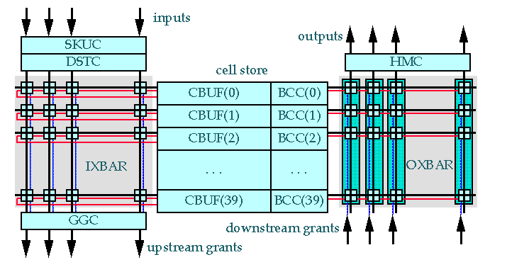
Arriving cells enter the switch element at the upper left, passing
through a Skew Compensation Circuit (SKUC) and a
Distribution Circuit (DSTC) before entering the Input Crossbar
(IXBAR). The IXBAR forwards cells to free buffer slots in the central
Cell Buffer (CBUF). Each row of the CBUF stores one cell
(actually one fourth of the cell, plus control information) and has an
associated Buffer Control Circuit (BCC). Outgoing cells pass
through the Output Crossbar (OXBAR) and Header Modification
Circuit (HMC) before proceeding to the output. Downstream neighbors
provide a one bit flow control signal each cycle, indicating if they
are prepared to receive an incoming cell or not.
These grant
signals are used within the (OXBAR) to control
the flow of cells from the CBUF to the outputs.
Upstream grants
are generated by the Grant Generation Circuit (GGC)
based on the number of available CBUF slots. The CBUF has been
dimensioned to hold 40 cells.
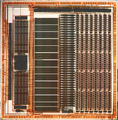
The switch element is implemented using four chips, each of which handles
eight bits of the 32 bit data path. The switch element chip, shown at right
has been
fabricated in a 0.8 micron, 3.3 volt CMOS process.
The data flow through the chip is from left to right, with skew
compensation on the periphery at left, followed by a block that
includes the input crossbar split into an upper and lower half
surrounding the DSTC. The dense section that runs from top to bottom
just left of center is the CBUF and the BCCs are immediately to its
right. The large area to the right of the BCCs is the OXBAR. The chip
has approximately 650,000 transistors. The design was specified using
VHDL and designed using industry-standard synthesis tools and a
standard cell library, using conservative engineering rules
to allow for process variations and variations in operating
temperature and power supply voltage.
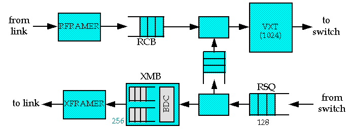
Port Processor
The Port Processor (both input and output sections) is shown below.
Cells coming from the external link enter a Receive Framer
(RFRAMER) driven by the recovered clock from the link
and enter a Receive Buffer (RCB) while awaiting transmission to
the switch. When the switch is prepared to accept a cell, it is
transferred from the RCB, through the Receive Circuit to the
Virtual Path/Circuit Translation Table (VXT) which provides the
routing information needed by the switching network. Cells coming from
the switch to the link pass first through a Resequencer (RSQ) and
then through the Transmit Circuit (XMIT) to the Transmit
Buffer (XMB).
Cells proceed from there to a Transmit Framer (XFRAMER) and
the external link. The XMIT circuit can also direct cells to a
Recycling Buffer (CYCB).
Resequencing Cells
The resequencer ensures that cells, which may follow different paths
through the switching network and be delayed by different amounts of
time, are restored to their original order before transmission on the
external links.
It uses a timing-based resequencing method. Cells
being sent from an IPP to the switching network are time-stamped with
their time of entry (placed in the cell's Timestamp field (TS)).
When cells emerge from the switching network, this time stamp field is
used to determine the cell's age (which is defined as the time
that has elapsed since it entered the switching network). Cells are
released from the resequencer in `oldest-first' order, but not until
their age reaches a system-dependent age threshold, which is set
to the maximum delay that cells can be expected to encounter in the
switching network (for systems with up to 4,096 ports an age threshold
of 64 cell times is ample). In a switch that uses cell recycling for
multicast, the resequencing mechanisms must also compensate for the
potential misordering that can occur when reconfiguration of a
multicast connection causes cells that pass through the connection
right after a reconfiguration to experience one fewer pass through
the system than cells that go through just before the reconfiguration.
This is handled using a transitional time stamping mechanism in
the IPP. This mechanism causes the time stamps of cells arriving right
after a reconfiguration to be artificially inflated (making the cells
appear `younger' than they really are) causing them to be delayed
longer at the outgoing resequencer. This allows cells that went through
before the reconfiguration a chance to catch up. The added delay is
smoothly reduced over a short period of time (10--20 microseconds in the
WUGS switch), causing only a momentary irregularity in the flow of
cells through the connection.
Congestion Control
The port processor implements several simple mechanisms to control the
effects of congestion. First, the XMB, where most cell queueing occurs
in the system, provides separate buffers for reservation-oriented
continuous stream traffic and bursty discrete stream traffic.
Cells are identified as belonging to one or the other class through a
Continuous Stream Bit (CS) inserted in arriving cells by the VXT.
The continuous stream traffic includes both constant bit rate and
variable bit rate traffic with modest peak-to-average rate variations,
while the discrete stream category is intended for bursty data traffic
with high variability and greater tolerance for delay. The continuous
stream queue is strictly higher priority than the discrete stream
queue.
In addition, the XMB implements a simple block discard mechanism on
selected virtual circuits, which performs block discarding on the basis
of AAL 5 frames, rather than on individual cells. The particular
algorithm used is a variation of the well-known Early Packet
Discard technique in which hysteresis is added to damp the
oscillations that can otherwise occur, making it possible to achieve
100\% throughput with modest buffer sizes.
The block discard is implemented through the use of a Block
Discard Index (BDI) which is inserted into arriving cells at the VXT. A
non-zero BDI indicates a virtual circuit on which block discarding can
be performed. The index is used by the Block Discard Controller
in the XMB to access one bit of state information that controls the
discarding of cells for that virtual circuit.
While the switching network has sufficient bandwidth to ensure that
cells normally proceed to the output port for buffering without
congesting the switching network, sustained high rate bursts can lead
to congestion in the switching network that will ultimately back up to
the input ports, causing the RCBs to fill up and exceed a preset
threshold. If this happens at a particular IPP, it begins discarding
all received cells with CLP=1 or CS=0 and continues discarding these
cells until a timer has expired. The timer is generally set with a long
enough period to ensure that the congestion has time to clear completely.
This is a fairly drastic response to an event which should
occur very rarely in a network which is properly engineered and controlled
at higher levels.
Control Cells
The chip set has been designed to allow control from a remote
processor. In particular, for any link on which the feature is enabled
(through a hardware switch), cells received with a VPI field of 0 and
VCI field of 32 are interpreted as control cells, with the payload of
the cell specifying the desired control action. Options include
reading and/or writing entries from the VXT in any port processor and
accessing a variety of hardware registers in the IPPs and OPPs. These
include hardware counters that record the total number of cells passing
over different data paths, the number of cells discarded
due to HEC errors, buffer overflows or various error conditions. There
are also registers controlling the resequencer age threshold, the low
priority cell discard thresholds for various buffers, the VXT bounds
register and other variables that affect the switch's operation.
Transmission Interfaces and System Configurations
The port processor chips have been designed to accommodate a variety of
different transmission interfaces. In particular, the chips implement
the 16 bit Utopia interface standard for SONET transmission interfaces
and a 32 bit extension of that standard. This allows them to interface
easily to current OC-3C and OC-12C transmission interface chips and to
future OC-48C devices.
The port processors can also accommodate interfaces using a simple
serial data link chip set produced by Hewlett Packard (G-link). These
interfaces can be operated at data rates of more than 1.2 Gb/s and are
currently less expensive than OC-12C devices (roughly one-fourth the cost).
The port processors also
support a special dual G-link mode in which cells are sent at 2.4 Gb/s
over a pair of G-links in parallel. When operated in this mode, the
receiving IPP synchronizes the incoming streams to recover the
transmitted data. The synchronization mechanism accommodates
skew of about 12 ns, so the fiber lengths can differ by no more than
about two meters. The dual G-link interface is intended primarily to
permit demonstration of 2.4 Gb/s switch operation in the absence of
commercially available OC-48C framer chips.
While not a substitute for a true 2.4 Gb/s link,
it can be useful in certain specialized applications.
WUGS-20 Physical Packaging
A 20 Gb/s capacity system (designated WUGS-20) is being built at
Washington University currently. These systems have
eight ports on the core fabric. Each of these eight ports can accept
line cards supporting several different transmission interfaces.
The kit distribution will include six line cards supporting
an interface speed of 1.2 Gb/s
based on Hewlett-Packard serial data link chips (called G-link
chips). The other two ports will come equipped with OC-3 interfaces,
probably with two OC-3 interfaces on each line card, although the
plans for this have not been finalized yet.
Line cards are also being designed for OC-12 and OC-48 interface speeds.
These will not be included in the core kit distribution, but may be
made available for purchase.
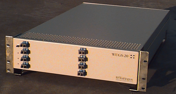
The photograph above shows the WUGS-20 switch packaging.
The switches are rack-mountable (or can be
simply placed on a desktop) and will be about 11 cm tall.
Connections will be through the front panel, which can be customized
for different line card configurations.
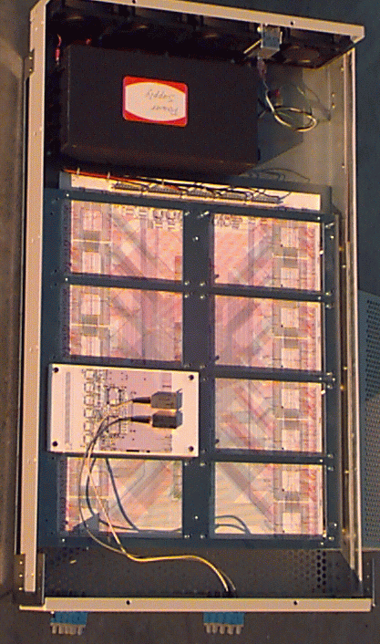
This photo shows the internals of the WUGS-20 switch (looking straight
down from the top with the cover removed) using mock-ups
of the internal components. The switch elements, IPPs and OPPs will
be mounted on a large circuit board, a mock-up of which can be seen
at the bottom of the enclosure. You can see the PGA sockets where the
IPP and OPP chips will be mounted along the left and right sides of the
board mock-up. Line cards sit above this main board,
connecting to it using connectors at the left and right edges of the
enclosure. A mock-up of one line card is shown in the photo, along with
optical modules, which connect to the front panel connectors via fiber optic
pigtails. The main board and line cards are mounted on a central metal
plate that can be seen in the figure, using stand-offs.
The power supply is at the rear of the enclosure and power connections
are made to the rear edge of the main board. There is also a set of
fans at the rear of the enclosure which draw air through the enclosure
to cool the components.
The enclosure was designed to be taller than needed for the standard
line cards, so that experimental line cards needing more board real estate
could be accommodated within the enclosure. Typically, these cards with
have the same dimensions as a standard card, but will also have a
mezzanine card that sits above the base card. These mezzanine cards may
extend over a larger area, within the enclosure, if need be (occupying
space above the other standard line cards).
Scaling Up to Larger Sizes
Plans for larger configurations have been developed, and Washington University
is actively seeking partnerships with commercial firms interested in
supporting the implementation of such larger systems.
The figure below shows a system with 64 ports on the core switch,
giving it a throughput of up to 160 Gb/s.
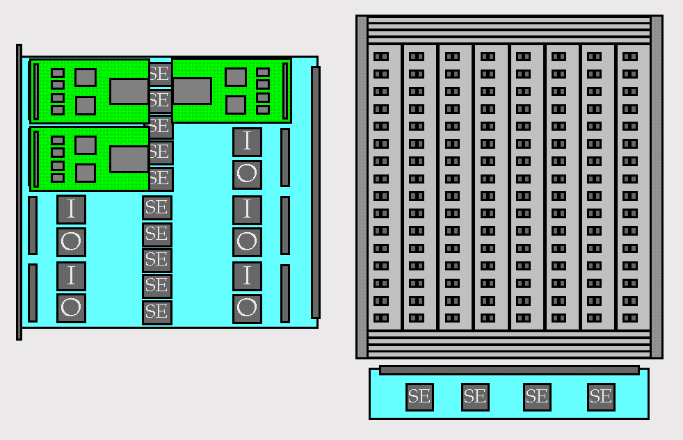
This system would be made up of eight I/O modules, each containing a large
circuit board hosting two switch elements (eight chips) and eight port
processors (16 chips), together with eight line cards, each containing
two 1.2 Gb/s interfaces.
These would connect to a backplane
that would provide connections to a set of small cards at the top that
would carry the switch element chips constituting the center stage of
the required three stage network. Such a system could be packaged in a
rack-mountable unit, approximately 75 cm in height with fiber
connections through a front panel.
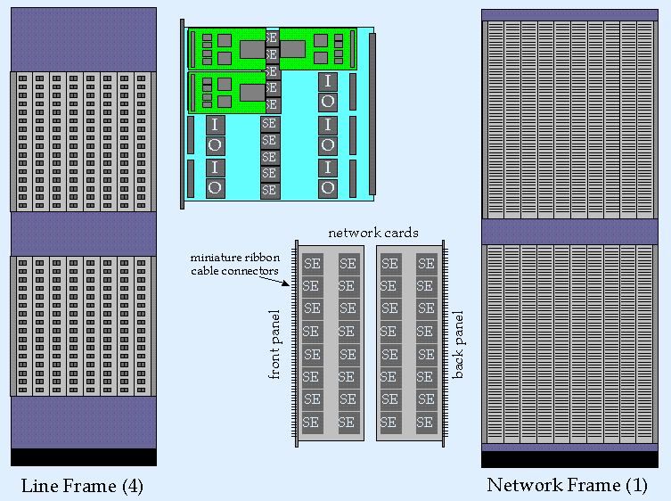
Still larger systems can be
constructed using subsystems similar to this. The figure above shows
components that can be used for systems with a capacity of up to 1.2 Tb/s.
This system could be implemented in five standard equipment racks.
For More Information
The references given below provide further details on Washington University's
gigabit switching technology. Additional information can be obtained by
contacting Jonathan Turner, email: jst@cs.wustl.edu, phone: 314-935-6132,
FAX: 314-935-7302.
-
``Design of a Gigabit ATM Switch,''
WUCS-96-07, 2/96.
-
``An Optimal Nonblocking Multicast Virtual Circuit Switch,''
Proceedings of Infocom, June 1994, pp. 298--305.
-
``Maintaining High Throughput During Overload in ATM Switches,''
Proceedings of Infocom, 3/96.
-
``Multicast Virtual Circuit Switch Using Cell Recycling,''
U. S. Patent #5,402,415, March 28, 1995.
-
``Data Packet Resequencer for a High Speed Data Switch,''
U.S. Patent #5,339,311, August 1994 and
U.S. Patent #5,260,935, November 1993.
Acknowledgements. This work has been supported by a major contract
from the Advanced Research Projects Agency and a grant from the National
Science Foundation.
Prepared by
Jonathan Turner: jst@cs.wustl.edu. Last updated 3/4/96.
 This site included in
InterNIC Academic Guide to the Internet.
This site included in
InterNIC Academic Guide to the Internet.