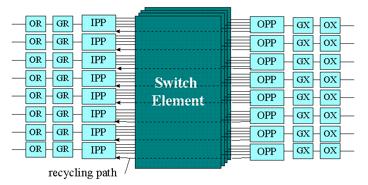
The figure given above is a block diagram of the eight port ATM switch that is included with the gigabit network kits. At the core of the switch is an eight port, shared buffer switch element made up of four chips, each of which switches an eight bit portion of the 32 bit wide internal data paths. Since the 32 bit data paths are clocked at a rate of 120 MHz, the raw data throughput is over 30 Gb/s. Internal overhead in the switch reduces this to a usable data rate of 25.4 Gb/s or about 3.2 Gb/s per port, making the system fast enough for external links of up to 2.4 Gb/s while operating at an occupancy of 75%. The switch element can accept cells with a pair of output addresses and is designed to forward copies of the cell to both specified outputs, or optionally, to all outputs in the range bounded by the specified outputs. The copied cells can (optionally) be recycled back to the corresponding input ports, allowing an arbitrary number of copies to be produced from a single input cell.
ATM port interface functions are provided by two additional chips, the Input Port Processor (IPP) and the Output Port Processor (OPP). The IPP includes a virtual path and virtual circuit translation table, used to determine the output port and new VPI/VCI for incoming cells. The OPP buffers cells awaiting transmission on the external links. The OPP and IPP are also linked by a direct data path which is used to allow cells to be recycled through the fabric multiple times to enable multicast transmission. This recycling data path, used in combination with the copy-by-two capability of the switch allows a multicast virtual circuit with f distinct outputs to be implemented using log2f passes through the switch.
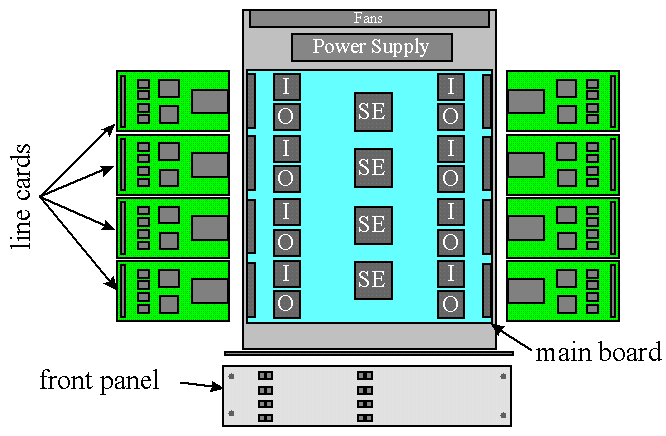
The diagram above shows the physical packaging of WUGS-20 switches (the 20 indicates 20 Gb/s capacity) that are being distributed with the gigabit kits. A single main circuit board contains all the ATM components, while the transmission interface circuits are on separate line cards. The kit distribution includes six line cards supporting an interface speed of 1.2 Gb/s based on Hewlett-Packard serial data link chips (called G-link chips). The other two line cards come equipped with a pair of OC-3 interfaces. Line cards are also being designed for OC-12 and OC-48 interface speeds. These will not be included in the standard kit distribution, but may be made available for purchase.
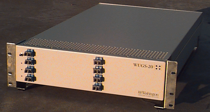
The photograph above shows the WUGS-20 switch packaging.
The switches are rack-mountable (or can be
simply placed on a desktop) and will be about 11 cm tall.
Connections are through the front panel, which can be customized
for different line card configurations.
The enclosure is designed to be taller than needed for the standard
line cards, so that experimental line cards needing more board real estate
can be accommodated within the enclosure. Typically, these cards with
have the same dimensions as a standard card, but will also have a
mezzanine card that sits above the base card. These mezzanine cards may
extend over a larger area, within the enclosure, if need be (occupying
space above other standard line cards).
Although the prototype switches support only eight ports, the chip set implements a general architecture that can support up to 32,768 ports at rates of up to 2.4 Gb/s each. Larger configurations are constructed by combining switch elements in multistage configurations. For example, a 64 port switch requires a three stage configuration with eight switch elements per stage. A 512 port switch requires a five stage configuration with 64 switch elements per stage. In general, for k between 1 and 5 an 8k port switch requires 2k-1 stages with 8k-1 switch elements per stage. Such a system provides 8k-1 different paths between each input and output port and the switch elements are designed to distribute traffic evenly over all the alternate paths, in order to obtain maximum efficiency. This dynamic load balancing technique, in combination with the cell recycling approach to multicast yields a nonblocking multicast switch architecture with optimal scaling properties, allowing systems with thousands of ports to be implemented for approximately the same cost per port as small systems.
The switch is designed to be remotely controlled by sending cells to it over any of its ports on a designated control virtual circuit. Through this mechanism, a remote control processor can read and write the virtual path and virtual circuit tables in the IPPs, access counters (per VP/VC cell counters, buffer overflow counters, HEC error counters, etc.) and hardware configuration registers in the IPP and OPP, and enable or disable individual links. This separation of the control from the switching allows for greater flexibility (there's no constraint on the type of computer used for control or its location in the network) and allows the amount of control capacity to be configured independently of the amount of switching capacity. In specialized applications, it's even possible for user workstations to directly manipulate switch control tables (presumably using an appropriate distributed control protocol), allowing more rapid configuration of virtual circuits on behalf of applications.
More information on the switch architecture and detailed design can be found in the following references.
Prepared by Jonathan Turner: jst@cs.wustl.edu. Last updated 8/21/97.