|
CSE/CoE 535
|
Acceleration of Algorithms in Reconfigurable
Hardware
|
Lockwood, Fall 2003
|
Homework Assignment 1
Assigned: Wednesday, August 27th, 2003
Due: Wednesday, September 3rd, 2003 before 4pm
(35
points)
Complete Homework
Use the document editor of your
choice to electronically generate solutions to your homework.
Submit Solutions: A paper copy may be turned in before class starts,
or given to Jing or Mike in Bryan 426.
Reading/Reference Material
Homework Questions
Part 1. FPGA Design and VHDL Review
- Define the following terms. Spell out the acronym (where needed) and provide a short definition. (1 point each)
- ASIC
- FPGA
- CLB
- Synthesis
- VHDL
- RTL
- Signal
- Event
- CSAs
- Sequential statement
- FSM
- Sensitivity list
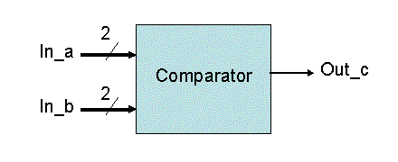
- Implement the 2-input comparator illustrated below in a Xilinx LUT.
Note that the inputs are each 2 bits wide (for a total of 4 inputs). When in_a equals in_b, out_c = '1'. Otherwise out_c = '0'. Following the example shown in Figure 3-8 on page 39
of Yalamanchili,
draw the gate-level schematic diagram and show how you map the circuit to a Xilinx 16x1 LUT. (3
points)

Figure 1: Interface of a 2-input comparator.
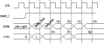
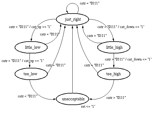
- Provided below is a sample state machine and counter, along with a bubble
diagram of the state machine.
- Analyze the provided code, referring to the state machine bubble
diagram as necessary.
- Fill in what state the finite state machine is in for parts (a)
through (d) (2
points)
- Fill in what value cntr has for parts (e) through
(g) (2
points)

Figure 2: Timing Diagram for Problem 3.

Figure 3: State Machine bubble diagram for Problem 3.
- Read Chapter 4 of Yalamanchili and do exercise 4.2 Step 1 and Step 2 on page 70. (3
points)
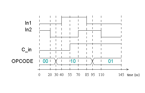
Assume that when OPCODE = "00", the upper input to the Mux is selected; when OPCODE
= "01", the middle input to the Mux is selected; the lower input to the Mux is selected when OPCODE takes other values.
Given the following input waveforms, draw the waveforms for the Result and c_out signals.

Figure 4: Input waveform.
- Read Chapter 8 of Yalamanchili and do Exercises 4 and 5 on page 248. (4
points)
Part 2 Protocol Wrappers
The Protocol Wrappers
provide an abstraction of ATM-based cell processing in order to format input
data. In
this way, our application can focus on processing data at the IP layer. In order to process
packets, the wrappers provide the following interface to the application, as
shown in the Figure 5 below.

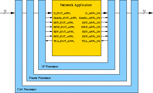
Figure 5: The Layered Protocol Wrappers - IP Layer
Interface
Of interest to us are the signals labeled on
the input side of the network application (the left side). A brief
description of the signals follows.
D_OUT_APPL – This is a 32-bit vector of incoming packet
data. Our applications will always operate on 32-bit words.
DataEn_OUT_APPL – When this signal is asserted, the
value on D_OUT_APPL is valid. This signal is VERY important
and must always be checked prior to operating on data from
D_OUT_APPL.
SOF_OUT_APPL – This signal is pulsed at the beginning
of a packet to indicate the start of a frame.
SOIP_OUT_APPL – This signal is pulsed at the beginning
of the IP packet header. Upon the arrival of the version / header
length / type of service / total length word of the IP header, this
signal is asserted.
EOF_OUT_APPL – This signal is pulsed to indicate the
end of the current frame, that is this will be pulsed upon the
arrival of the last word of an IP packet.
SOP_OUT_APPL – This signal is pulsed when the first
word of an IP packet's data is available on D_OUT_APPL. In the case
where the packet is an UDP packet, this signal will be pulsed when the
UDP port word is available.
TCA_OUT_APPL – This signal is used as congestion
control. When asserted (NOTE: this signal is asserted low '0'), the
network application is communicating that it can no longer accept
data from the IP wrapper interface until it has available space.
This signal will be asserted when input buffers are full (i.e. the
network application is backlogged).
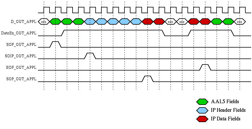
Figure 6 shows a possible timing scenario of these signals when a
packet arrives at the network application.

Figure 6: IP Wrapper signal timing.
Some things of interest about Figure 6:
The amount of AAL5 header fields is variable. Thus, the
assertion of SOIP_OUT_APPL must be examined.
The amount of IP header fields is variable due to the
possibility of specifying options. Thus, the assertion of
SOP_OUT_APPL must be examined.
The assertion of DataEn_OUT_APPL must always be checked to
ensure valid data is sitting on D_OUT_APPL. Note that in the middle
of the packet data, it is de-asserted, signifying the data is not
valid. Two cycles later, it is reasserted to specify valid data is
arriving on D_OUT_APPL.
The issuance of EOF_OUT_APPL signifies the last valid word of
packet data. Following this assertion, there are two words of AAL5
trailer that arrive. For our purposes, these two trailer words can
be ignored.
You will become very familiar with the IP Wrappers in this class, so
it is good to introduce them here. In addition, this will help you in
determining what the state machine below is doing.
- Describe the significance of the wrapper interface signal 'dataen_out_appl'. (2
points)
- Read
Chapters 6 and 7 of Yalamanchili as reference to analyze the
cpp_rules_programmer found here.
Draw a bubble diagram, similar to that of problem 3 (i.e. similar to
Figure 3), of the state machine as is. Mark all
transition conditions and output assignments. (3
points)
Explain why the 'clk' signal is not found in the sensitivity list of
the process named nextstate nor outputs. (2
points)
Describe how 'soip_out_appl_int' is used within cpp_rules_programmer.vhd. (2
points)
