|
CSE/CoE 535 |
Acceleration of Algorithms in Reconfigurable Hardware |
Lockwood, Fall 2003 |
Use the document editor of your choice to electronically generate solutions to your homework.
Submit Solutions to: Electronic Homework Server
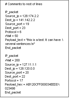
In this semester, all network traffic we deal with is IP traffic. It is assumed that you are familiar with IPv4 packet format. Most of the time, you will need to generate your own IP traffic to test your circuits. The following sample file (Figure 1) specifies two IP packets. The first one is a TCP packet (Protocol = 6) and the second one is a UDP packet (Protocol = 17).

Figure 1: A sample .spc file specifying two IP packets. Comments start with # sign and are at the beginning of each packet specification. IP_packet, Source_ip, Dest_ip, Source_port, Dest_port, Protocol, Wait, Payload_text, Payload_hex, and End_packet are key words. A key word must be the first word in the line. All key words are case sensitive and can show up in any order. Each key word specifies a field in the IP packet. A equal sign "=" follows the key word and then the specification. Space is allowed before and after "=". If the specification cannot be fitted in one line, a backslash "\" must appear at the end of line indicating more information is followed at the next line. Certain charaters are represented by escape sequences, such as \n (newline), \r (carriage return), \t (horizontal tab), and \\ (backslash). Payload_text specifies a text payload inside a pair of double quotes. Payload_hex specifies a hex payload (Note that there are no double quotes). Except that the payload specification can be either text or hex, all the other specifications must be representated as decimal numbers. If no specification is associated with key word "Wait", "Payload_text", or "Payload_hex", this key word shouldn't appear in the packet specification. For example, if a packet has no payload, neither payload_test nor payload_hex should appear in the packet specification. Blank line(s) can appear inside or outside each packet specification. Key word "Wait" specifies how many wait cycles are needed between the current packet and the previous one. The number of wait cycles allowed are: 10, 50, 100, 200, 500, and 1000.
A testbench that mimics the IP wrapper introduced in Homework 1 will be provided to you. It interfaces with the user application just like the IP wrapper does. An input file named input_ip.dat contains the IP traffic in the format shown in Figure 2. The testbench reads the input file and sends data and control signals to the user application. If IP packets are generated in the user application and needs to be sent out, the testbench will write the packets into an output file called output_ip.dat. The input_ip.dat and the output_ip.dat are in the same format. Files in this format are hard to read, which is where you come in.
Write a program in C, C++, JAVA or Perl to do the conversion from the file format of Figure 1 (.spc) to the file format of Figure 2 (.dat). Note that the file in Figure 2 is generated from the file of Figure 1. You can download both of them here: input_ip.spc and input_ip.dat. You can use them to test your code. You may notice that files in .spc format do not provide enough header information used to generate corresponding files in .dat format. Since the testbench is used only for simulation purposes, not all fields in the header matter to the user application, such as header checksums. Our application will not check such fields, since the IP wrapper component takes care of them. Figure 3 shows the fields (green) in the header that should be taken care of when you do the conversion (We call them do-care fields). The rest do-not-care fields (blue) can be filled in whatever value you want, but zeros will suffice. In Figure 2, the do-care fields and payloads are highlighted with an underscore.
|
|
|
|
Figure 2: File format (.dat) used by testbench. No blank line is allowed anywhere. "IPpacket" and "wait" is case sensitive keywords. Each line is either a 8 character word or a 32-bit word in Hex (case insensitive). In .dat, the number of wait cycles is specified using "wait" key word. Underscore(s) are inserted between "wait" and the number when needed. |
Figure 3: IP, UDP and TCP header format. Fields in green color are the do-care fields. The rest field in blue color are the do-not-care fields. Since "Options+ padding" fields in the IP header and TCP header won't be used at the simulation stage, "IHL" in the IP header and "Header length" in the TCP header will always be 5. |
When converting files from .dat to .spc, you should pay attention to the packet payload. If the payload is all printable ASCII characters (ASCII code is in the range from 32 to 126) or the escape sequences shown above, you must convert them to text using key word payload_text. If any one byte is neither a printable ASCII character nor an escape sequence, you should convert the entire payload to hex numbers using key word payload_hex. For example, you can convert the payload of packet #1 to text and that of packet #2 to hex.
The snort-on-a-chip module you will design for this class will be implemented on a Xilinx XCV2000E FPGA. This FPGA has 160 4096-bit Block RAM components. In this assignment, you will utilize two of these components, described below.
We will utilize the dualport feature of this block RAM, allowing us to read and write the memory contents from different ports. The interface for the device can be seen in Figure 4.
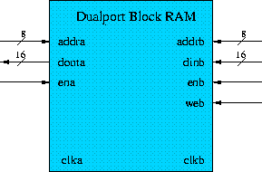
Figure 4: Dualport Block RAM signal interface.
The block RAM has been created, using Xilinx Coregen, to have 256 different entries, with 16-bits held within each entry. Port A will be used to read memory contents, while Port B will be used to write memory contents. In order to read from memory, the ena signal must be asserted while the entry to read is placed on addra. To write to memory, the enb and web signals must be asserted, and the entry to write to along with the data to write must be placed on addrb and dinb, respectively. A simple timing diagram for this component can be found in Figure 5.
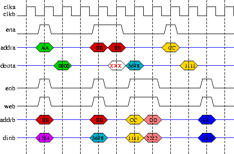
Figure 5: Block RAM timing.
Note that if you read from and write to the same location on the same clock cycle, the value read from memory is invalid.
You task is to design a statistics counter using the above block RAM component. The proposed interface is as shown in Figure 6.
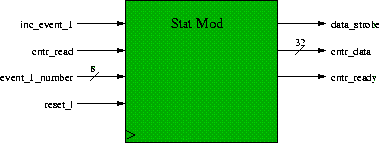
Figure 6: The interface to be used for the statistics counter.
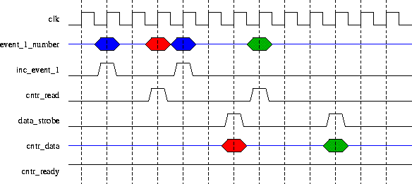
Figure 7: A sample timing diagram of the functionality of the component.